
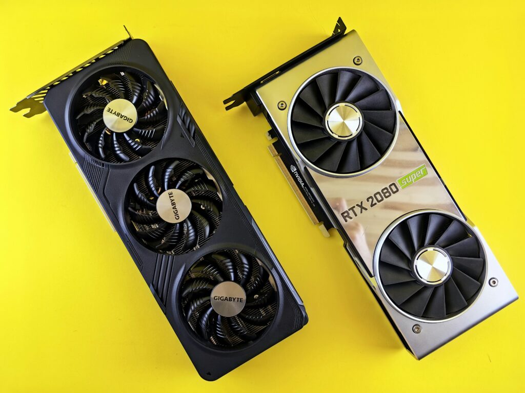
The Dawn of the Blackwell Era
On March 18, 2024, at the GTC conference, Nvidia unveiled its Blackwell platform, named after David Harold Blackwell, the first African American inducted into the National Academy of Sciences. This isn’t just another incremental speed boost; it is a fundamental redesign of how GPU compute is handled at scale. By utilizing 208 billion transistors on a dual-die configuration, Blackwell aims to drastically reduce the energy consumption and operational costs associated with large language model (LLM) training.
Technical Specifications and Throughput Capabilities
The core innovation lies in the second-generation Transformer Engine. This feature enables the system to support higher levels of precision, including 4-bit floating point, which effectively doubles the model sizes that can be computed without sacrificing accuracy. According to official data from Nvidia’s official press release, the Blackwell B200 GPU provides up to 30x the performance in AI inference workloads compared to the previous H100 architecture while simultaneously reducing power consumption by up to 25x.
Impact on Enterprise AI Workflows
For consultants and businesses, the primary bottleneck in scaling automation has always been the sheer cost and latency of compute. With Blackwell, the transition from prototype to production becomes significantly more streamlined. If you are currently managing complex automation pipelines, integrating this hardware into your cloud infrastructure strategy could mean the difference between real-time data processing and delayed execution. You can read more about optimizing your current digital infrastructure in our recent piece on optimizing enterprise workflows.
Expert Analysis: The Future of Compute
Industry analysts have noted that the Blackwell architecture is heavily focused on multi-GPU scalability. By utilizing the fifth-generation NVLink, the chips can communicate at 1.8 terabytes per second, allowing multiple Blackwell chips to act as a single, unified GPU. This level of interconnectivity is the key to training next-generation models that exceed trillion-parameter scales. As experts, we anticipate that this hardware will become the gold standard for private cloud AI environments over the next 24 months.
A Path Toward Sustainable Scaling
The industry is moving toward a more sustainable footprint. While Blackwell requires substantial power, its efficiency per watt is an industry-leading benchmark. Companies that invest in this generation of hardware are not just buying speed; they are future-proofing their data centers against the rising costs of energy-intensive AI training. We expect initial enterprise adoption to be focused on sectors requiring heavy data analysis, such as finance, healthcare, and predictive manufacturing.