
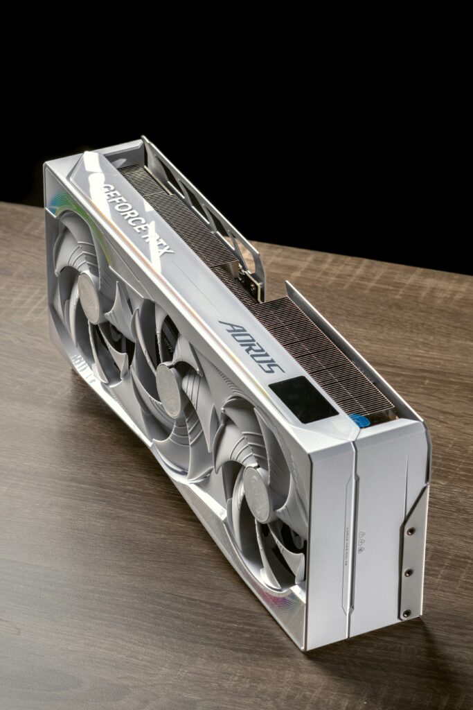
The Emergence of the Blackwell Architecture
In mid-2024, Nvidia officially began rolling out its highly anticipated Blackwell architecture, marking a pivotal moment in the evolution of silicon design. The platform, named after David Harold Blackwell, the first African American scholar inducted into the National Academy of Sciences, focuses on solving the challenges of massive-scale parallel computing. Unlike traditional incremental upgrades, Blackwell represents a fundamental rethink of how data passes through memory and logic units.
The announcement of these GPUs has sent ripples through the industry, with hyperscalers and enterprise data centers scrambling to integrate the new hardware. According to official reports from The Verge, the architecture integrates two-die GPU designs to effectively double the transistor count, pushing the boundaries of what is physically possible with current lithography techniques.
Technical Breakthroughs and Industry Impact
At the core of the Blackwell platform is the second-generation Transformer Engine. This innovation allows the hardware to dynamically adjust precision—switching between FP8 and FP4—to optimize speed without sacrificing accuracy. For industries reliant on heavy simulations and large-scale data processing, this means faster time-to-insight. We have previously explored how hardware infrastructure dictates operational efficiency in our guide to optimizing enterprise workflows.
The impact is profound: organizations can now train models that were previously considered prohibitively large or slow to compute. This is not merely an increase in raw speed; it is an improvement in power efficiency per watt, a critical metric for companies committed to reducing their carbon footprint while scaling their digital operations.
Expert Analysis and Future Projections
Industry analysts remain bullish on the long-term potential of the Blackwell series. By reducing the communication overhead between processors, Nvidia has effectively addressed one of the most persistent bottlenecks in cluster computing: latency. As we look toward the next three to five years, it is expected that Blackwell will become the backbone of the most advanced research labs and corporate innovation centers globally.
However, it is important to maintain a balanced perspective. While the raw specs are revolutionary, the true value lies in the accompanying software ecosystem. Companies must consider the integration complexity; transitioning to a new hardware standard requires careful planning and a robust strategy to ensure that internal workflows are not disrupted during the deployment phase.
Conclusion
The Nvidia Blackwell architecture is more than just a component upgrade; it is a catalyst for the next wave of industrial digital transformation. As these chips become more widely available, the competitive advantage will shift toward companies that can effectively map their operational needs to this new level of computing power. Staying informed is the first step toward effective adoption.